.
Analysis of 3D stacked fully functional CMOS Active Pixel Sensor detectors
The IC technology
trend is to move from 3D
flexible configurations (package
on package, stacked dies) to real 3D ICs.
This is mainly due to i) the increased
electrical performances and ii) the cost of
3D integration which may be cheaper than to
keep shrinking 2D circuits. Perspective
advantages for particle tracking and vertex
detectors applications in High Energy
Physics can be envisaged: in this work, we
will focus on the capabilities of the
state-of-the-art vertical scale integration
technologies, allowing for the fabrication
of very compact, fully functional, multiple
layers CMOS Active Pixel Sensor (APS)
detectors.
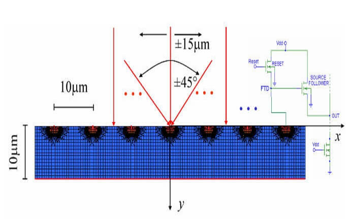
The main idea is to
exploit the features of the 3D
technologies for the fabrication of a
“stack” of very thin and precisely aligned
CMOS APS layers, leading to a single,
integrated, multi-layers pixel sensor. The
adoption of multiple-layers single detectors
can dramatically reduce the mass of
conventional, separated detectors (thus
reducing multiple
scattering issues),
at the same time allowing for very precise
measurements of particle trajectory and
momentum.
As a proof of concept,
an extensive device and circuit simulation
activity has been carried out, aiming at
evaluate the suitability of such a kind of
CMOS active pixel layers for particle
tracking purposes.)
Cite as
D. Passeri, L. Servoli, S. Meroli “Analysis of 3D stacked fully functional CMOS Active Pixel Sensor detectors” 2009 JINST 4 P04009
Leave a comment