.
A combined approach to the simulation of ionizing radiation effects in silicon devices
Silicon devices (both pixels and
microstrips) have been widely used in the
past years in High Energy Physics
experiments and also in other applications
involving the detection of ionizing
radiation such as medical imaging and
dosimetry.
The
simulation of the silicon devices response
to ionizing radiation is an important step
needed to understand the performances in
terms of signal, noise, spatial and energy
resolution as a function of several
technology parameters like doping profile,
geometrical dimensions, bias voltage. These
simulations are routinely carried out using
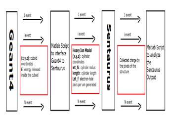
two separate approaches (and tools):
radiation interaction with a geometrically
segmented silicon material (GEANT4,
FLUKA, PENELOPE) taking into account the
physical processes and giving as output the
deposited energy; transport of generated
electron/hole pairs through the device with
electronic signal formation (SENTAURUS-TCAD).
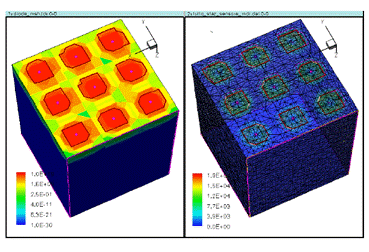
In
this work we propose a new combined approach
using both methods, applied to the case of
CMOS pixel sensor, to obtain a better
understanding of the behavior of the
devices.
Cite as
T. Ozdemir et al., A combined approach to the simulation of ionizing radiation effects in silicon devices, 2011 JINST 6 T0500, doi:10.1088/1748-0221/6/05/T05001
Leave a comment