.
Vertically Integrated CMOS Active Pixel Sensors for Tracking Applications in HEP Experiments
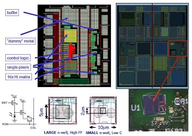
In this work we propose an innovative approach to particle tracking based on CMOS Active Pixel Sensors layers, monolithically integrated in an all-in-one chip featuring multiple, stacked, fully functional detector layers capable to provide momentum measurements (particle impact point and direction) within a single detector.
This will results in a very low material detector, thus dramatically reducing multiple scattering issues. A first chip prototype has been fabricated within a multi-project run using a 130nm CMOS 3D Chartered/Tezzaron technology, featuring two layers bonded face-to-face. Tests have been carried out on full 3D structures, providing the functionalities of both tiers and their inter-communications.
Actually, laser scans have been carried out using highly focused spot size, obtaining coincidence responses of the two layers. X-rays sources have been used as well for sensor calibration purposes.
Beam tests with 3MeV protons have been carried out at the INFN LABEC laboratories in Florence (Italy) to assess the suitability of the proposed approach for Minimum Ionizing Particle detection.
Cite as
D. Passeri et al., Vertically Integrated CMOS Active Pixel Sensors for Tracking Applications in HEP Experiments, IEEE Nucl. Sci. Symp. Conf. Rec. NSS12 (2012) 1330.
Leave a comment