CMOS Monolithic Active Pixel Sensors (MAPS) are charged particle tracking devices, integrating on the same silicon substrate a radiation sensitive detector element with its front-end readout electronics. Standard microelectronics CAD tools are used for their design and modern submicron or deep submicron commercial CMOS processes for the fabrication.
After production the device is directly ready to be employed without any use of complicated and expensive post processing like bump-bonding. Initially all prototypes of Monolithic Pixel Sensors were fabricated using a CMOS process version providing an epitaxial type of substrate. In this substrate type a thin (~10μm) lightly p-doped silicon epitaxial layer is grown on a heavily p++ doped thick (~500μm) supporting structure.
On top of the
epitaxial layer, structures of n+ and p+
wells are formed, providing surface for CMOS
transistors implantation (Fig.1). As result,
incoming beam after a thickness of material
shown a divergence greater than the initial.
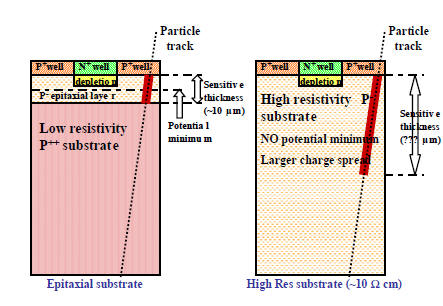
Fig
1. Cross section of silicon wafers used for
the fabrication of CMOS monolithic pixel
sensors. On the left, the structure of
epitaxial type wafer is shown. On the right
the non-epitaxial, high resistivity wafer is
presented.
In
the original MAPS implementation, this
epitaxial layer is used as a detector
radiation sensitive volume, with a diode
Nwell/Pepi working as a charge collecting
element [1]. The detector is only partially
depleted in the vicinity of the Nwell/Pepi
junction (1-2 μm
in depth), so the charge is collected mainly
through a thermal diffusion mechanism.
However due to the particular doping profile
(P++substrate/P-epi/P+well), there is a
potential minimum in the middle of the
epitaxy limiting the volume spread of
diffusing electrons created by the radiation
absorption.
These electrons may move only along the plane parallel to the surface and are rapidly collected when passing close to the collecting diode junction, with a typical collection time of the order of 100 ns. The detector active volume is limited in depth to the epitaxy layer only, because of the small lifetime of charge carriers inside a p++ substrate.
Therefore the total amount of
available charge created by an impinging
minimum ionizing particle amounts to a few
hundreds electrons only, for a typical
epitaxy thickness of the order of 10
μm. Several epitaxial
CMOS processes have been used in the past,
providing MAPS with rather outstanding MIP
tracking performances.
In the recent years even more MAPS are fabricated using a non epitaxial layer and an high resistivity substrate. The cross section of such a substrate is shown in Fig.1. In this case a supporting silicon wafer is uniformly p doped and is directly used as such for nwells and pwells implantation.
There is no potential minimum
in the bulk, therefore a larger charge
spread is anticipated. Contrary to epitaxial
substrate type, the sensitivity region has
no clear limit in depth and this effect
increase the total amount of charge
collected on the nwell/psubstrate diode,
compensating for a larger spread.
References
- D. Passeri et
al., Characterization
of CMOS Active Pixel Sensors for
particle detection: beam test of the
four sensors RAPS03 stacked system, Nucl.
Instr. and Meth. A 617 (2010) 573–575
- D.Passeri,et al. Tilted
CMOS Active Pixel Sensors for Particle
Track Reconstruction,
IEEE Nucl. Sci. Symp. Conf. Rec. NSS09
(2009) 1678. July 2006.
- L. Servoli et al. . Use
of a standard CMOS imager as position
detector for charged particles ,
Nucl. Instr. and Meth. A 215 (2011)
228-231,
10.1016/j.nuclphysbps.2011.04.016
- D. Biagetti et al. Beam test results for the RAPS03 non-epitaxial CMOS active pixel sensor, Nucl. Instr and Meth A 628 (2011) 230–233
- S. Meroli , Silicon pixel detectors for high precision measurements, PhD Thesis, Universita di Perugia, Italy (2012)
Anything missing? Write it here