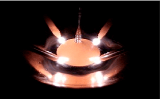
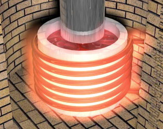
What is the meaning of discovery monocrystalline silicon made by Czochralski?
Jon Czochralski
discovered in 1916 what now is called
Czochralski Process, a process to growth large single
semiconductor crystals of exceptional quality
and for the production of silicon wafers.
Those can measure up to 2m by 0.5m and can be made
within 30 to 48 hours. Then they can be chipped off
in very thin sheets and used for the production of microprocessors
Czochralski made his discovery by accident in 1916 while
investigating the crystallization rates of
metals.
What has caused interest in his discovery after so many years ?
Czochralski method
was completely forgotten for years. In fact,
in the
first part of the last century it was used
mainly for studying the grow rate of some
metals.
However, after the war and the
discovery of the transistor,
scientists suddently became interested in the growth
of silicon.
In fact, the increasing demand
of semiconductor electronic materials in
1950 led the Americans G.K. Teal and J.B.
Little from Bell Telephone Laboratories to
rediscover and widely apply this growth
method, giving it a world-wide fame to the
Czochralski method as the best process to grow large single
crystals on an industrial scale.
The
natural growth process would take much long and would be limited to very small
sizes of crystals, making it unviable for
industrial production of electronic devices.
The level of miniaturization achieved today would be
otherwise impossible to
attain. Basically, computers would still be
the size of an entire room, instead of the
palm of your hand.
How the monocrystalline silicon is used today?
The Czochralski process
is the base of semiconductor chips.
In
fact the monocrystalline silicon form is
used extensively in solid-state devices, in
computers, and microelectronics industry due
to its incredible quality and the
total absence imperfections in the
silicon microstructure.
Without the
crystalline perfection, it would be
impossible to build high integrated devices
with millions of transistor-based circuits.
Monocrystalline silicon plays also an
important role in the photovoltaic
industries where high efficiency solar cells
use the sun’s light to produce water heating
as well as domestic and industrial electricity.
Even
at CERN, in all the experiments operating in
the LHC accelerator, silicon wafers grown
with Czochralski process are widely used.
Radiation silicon detectors grown with the Czochralski
process are considered to be one of the best
candidates for future high-energy
physic experiments due to their exceptional
quality and radiation hardness proprieties.
How Czochralski's discovery influenced the development of our civilization?
Large size silicon
monocrystals, grown with Czochralski
process, have been used for over 40 years
now as a standard material in semiconductor
industry all over the world. Some scientific
areas, such as the microelectronics, the
solid state physics as well as the material
science, which created the foundation of
modern technology, owe, at least in part,
their progress and present position to the
Czochralski's discovery.
His discovery
has proven vital for electronic revolution
as we know it today and it has been the key
for the computer diffusion that has brought
all the house Personal Computers
smartphones. From the perspective of almost
the past century the common opinion of the
scientific community recognized him as a
great scientist who has laid the foundation
for the development of the global
electronics.
Are you aware of any other discoveries and inventions made by Jan Czochralski?
It's not only on
crystals that Czochralski worked on. During
his entire professional life he was a very
active and competent scientist, able to
identify most important aspects of physical
problems, to understand them, and finally to
find successful application of the conceived
ideas.
As matter of fact he made
discoveries in metallurgy used for the
development of wheels that allowed trains to
go much faster than before.
Czochralski
was also a pioneer in what is now described
as technology transfer. He register a high
number of patents in Germany and Poland. In
addition during the war, when he worked at
the Technical University of Warsaw, he
developed an easily manufacturable grenade
for the Polish resistance.
To conclude,
history confirms that he was distinguished
scientist and inventor. It should be also
underlined that he had very modern views on
the role of engineering sciences. Much of
his research was driven by the needs of
industry and the search for new technologies
Do you think that the graphene production on an industrial scale is/would be a breakthrough similar to the silicon?
Both science and the
industry place high hopes in graphene.
It's considered as the wonder material of
our century with the power to revolutionise
micro-electronics. Just one atom thick, the
novel form of carbon is the world's thinnest
and strongest nano-material, almost
transparent and able to conduct electricity
and heat.
Graphene transistors would in
theory be able to run at faster speeds and
cope with higher temperatures than today's
classic silicon computer chips. That would
solve a fast-growing problem chip engineers
are facing: boost power and
shrink semiconductor size without
raising temperatures. Graphene's
transparency also means it could potentially
be used in touch screens and even solar
cells, and when mixed with plastics would
provide light but super-strong composite
materials for next-generation planes and
cars.
The problem so far came from a
lack of methods to grow it.
Single sheets of graphene are hard to
produce and even harder to make on an
appropriate substrate. While it is currently
possible to produce graphene layers,
relatively large ones can only be made on a
metal base. That hampers graphene's
electronics potential. Without such a base,
current techniques only allow for a maximum
layer surface of four square inches (25
square centimetres).
Now Polish
scientists, from the Institute of Electronic
Materials Technology claimed to discover a new method to produce entire
layers of graphene, a move that should help
to propel it out of the lab and push it into
everyday's life. This is an important step
forward on the path to the production of
transistors and then integrated circuits
made of graphene.
The great hope is that,
as happened to Czocharlski in the past, the
polish scientists can develop a new and
reliable production process that will
revoluzionize the world.
If there is a possibility to combine silicon and graphene? How?
Graphene poses a
significant challenge, though: in contact
with other materials it changes
significantly and loses its potential.
Some scientists were able to combine silicon
and graphene, in particular in the domain of
radiation detector. They were able to
combine graphene light detectors with
standard silicon chip.
The
super-conductivity and transparency of
graphene, could make it the ideal candidate
to produce super-efficient solar cells: it
does not stop incoming light rays and allows
electricity to move fast through its carbon
atom lattice.
This was achieved by
growing graphene on a copper foil, then
moving it to a glass substrate and coating
it with a silicon film. Measurements showed
that silicon-coated graphene has a power
conducting capacity 30 times higher than
traditional materials. This is an important
achievement that, however, still requires
lots of efforts.
But the big hope of
micro-electronic engineers is to use
graphene, combined with silicon, for future
CPUs working at 1THz — that means 1000GHz.
Also in this case, a big effort should be
put in place for the development of a
reliable industrial process capable to
combine graphite and other semiconductors.
References
- S. Meroli, Two growth techniques for mono-crystalline silicon: Czochralski vs Float Zone, (2012).
Anything missing? Write it here