Radiation detectors
made of silicon are cost effective and have
excellent position resolution.
Therefore, they are widely used for track
finding and particle analysis in large
high-energy physics experiments.
Exposure of the silicon material to
particle radiation causes irreversible
defects that deteriorate the performance
of the silicon detectors. Normally an
approach to improve the radiation hardness
of the silicon material is to increased
oxygen concentration in silicon material.
Exposure of the silicon material to particle radiation
Exposure of the silicon material to
particle radiation causes irreversible
defects that diminish the performance of the
silicon detectors. Thus, improving the
radiation hardness of the detectors is a
very important research subject in
experimental particle physics. Silicon
detectors are pn-junction devices operating
at full depletion. Radiation induced defects
diminish the performance of the silicon
devices in two principal ways.
First, in
the silicon material, the defects create generation-recombination
centres that decrease the minority
carrier diffusion length and increase the
leakage current with relation to the
irradiation dose. Thus, the electrical
signal created by the particle traversing
the detector becomes difficult to
distinguish from the background noise.
Second, lattice defects change the effective
resistivity of the silicon.
Consequently,
the operating voltage needed for the full
depletion of the detector changes and
gradually may exceed the breakdown voltage
of the device. Additionally, as the
irradiation dose increases, the defects
eventually change the type of conductivity
of the silicon from n-type to p-type.
The deterioration of the silicon detectors
in particle radiation is the most serious
limitation of the long-term performance of
large modern particle physics experiments.
Thus, all the results obtained in the
improvement of radiation hardness of
silicon detectors are directly applicable to
the international community of high-energy
physics, including future CERN experiments.
In addition, the results can be exploited in
space research since similar detectors are
used to measure high particle radiation
fields in space.
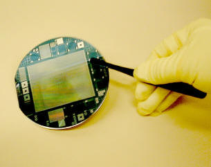
Fig 1.
Radiation detector and test structures
processed on a silicon wafer.
Why
high resistivity Czochralski silicon?
Silicon detectors have traditionally been processed using Float Zone silicon (Fz-Si) wafers. Fz-Si crystals are grown without quartz crucibles acting as a source of impurities, i.e. oxygen, carbon, or boron. The lack of impurities results in high purity and high resistivity of the bulk silicon. Because of the high resistivity, the detector can be fully depleted at reasonable operating voltages. However, Fz-Si has a low oxygen concentration. The oxygen concentration can be increased by prolonged high temperature drive-in oxygen diffusion.
Unfortunately,
some metallic contamination is always
present in quartz tube diffusion furnaces.
At elevated temperatures, the diffusion
velocity of many harmful metals is much
higher than that of oxygen. This in turn may
lead to an extensive process induced
contamination in the silicon wafers, unless
a careful quartz tube cleaning procedure is
practiced.
Silicon wafers grown using
the
Czochralski method intrinsically contain
high level of oxygen, typically 10^17 –
10^18 cm-3.
In addition, the depletion
voltage of the Czochralski silicon (Cz-Si)
detectors can be tailored either by
adjusting the oxygen concentration in the
silicon bulk during crystal growth or by
manipulating the thermal history of wafers
during the detector processing.
Furthermore, using Cz-Si as detector
material may offer economical benefits.
Cz-Si wafers are available up to a diameter
of 450 mm while Fz-Si wafers are typically
of diameter 150 mm or 200 mm. Thus, very
large area silicon detectors could be
manufactured, which in turn could result in
significant savings in the costs related to
front-end electronics, interconnection, and
module assembly.
Crystal growth of Czochralski silicon
In the Czochralski method, polycrystalline silicon fragments are melted inside a quartz crucible.
During the process, argon gas continuously flushes the interior of the crucible and the surface of the silicon melt. Silicon single crystals are grown by slowly pulling a crystal seed up from the molten silicon, thus developing an ingot. Later, wafers are cut from the ingot. Oxygen concentration is one of the most important parameters of silicon wafers. For example, oxygen precipitates bind unwanted metallic impurities present during the processing of silicon devices. Furthermore, stress induced during high temperature processing can lead to the formation of slip defects in the wafer.
The presence of oxygen stabilizes the wafer, and thus Cz-Si wafers are less prone to slip than Fz-Si wafers. During crystal growth, oxygen is dissolved into silicon from the quartz crucible. Most of the oxygen is dissolved as silicon monoxide and is flushed away by argon gas. Furthermore, the resulting oxygen concentration depends on the velocity of the silicon melt flow as well as on the rate of oxygen evaporation from the surface of the melt. All these parameters can be influenced in order to get a desired oxygen concentration in silicon ingot. Since the silicon melt is an electrically conductive liquid, the magnetic field is an effective way to moderate and control the melt flow.
The Magnetic Czochralski (MCZ) method has several advantages, e.g. reducing the erosion of the silica crucible and thus reducing introduction of impurities during crystal growth. In order to grow n-type silicon ingots, phosphorous dopant is added to the silicon melt in order to create desired donor states in silicon. However, boron is a common element in nature and thus easily drifts from quartz crucible to silicon melt during crystal growth. Since boron acts as an acceptor in silicon, the amount of unwanted boron is an important limitation to the magnitude of resistivity in ntype silicon.
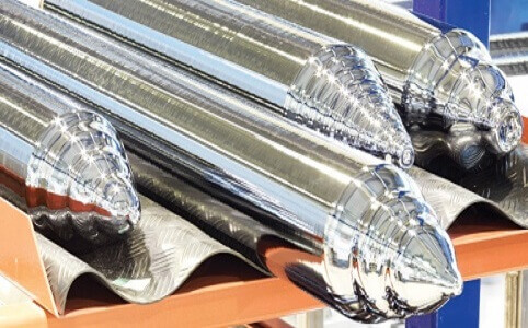
Fig 2.
Monocrystalline boules created using the
Czochralski process.
Conclusion
Anything missing? Write it here